
An uninformed perspective on TaihuLight's design
China’s new 93 PF TaihuLight system is impressive given the indigenous processor design and its substantial increase in its HPL score over the #2 system, Tianhe-2. The popular media has started covering this new system and the increasing presence of Chinese systems on Top500, suggesting that China’s string of #1 systems may be a sign of shifting tides. And maybe it is. China is undeniably committed to investing in supercomputing and positioning itself as a leader in extreme-scale computing.
That being said, the TaihuLight system isn’t quite the technological marvel and threat to the HPC hegemony that it may seem at first glance. The system features some some critically limiting design choices that make the system smell like a supercomputer that was designed to be #1 on Top500, not solve scientific problems. This probably sounds like sour grapes at this point, so let’s take a look at some of the details.
<h2>Back-of-the-envelope math</h2>Consider the fact that each TaihuLight node turns 3,062 GFLOPS (that’s 3 TFLOPS) and has 136.51 GB/sec of memory bandwidth. This means that in the time it takes for the processor to load two 64-bit floats into the processor from memory, it could theoretically perform over 350 floating point operations. But it won’t, because it can only load the two operands for one single FLOP.
Of course, this is an oversimplification of how CPUs work. Caches exist to feed the extremely high operation rate of modern processors, and where there are so many cores that their caches can’t be fed fast enough, we see technologies like GDDR DRAM and HBM (on accelerators) and on-package MCDRAM (on KNL) appearing so that dozens or hundreds of cores can all retrieve enough floating-point operands from memory to sustain high rates of floating point calculations.
However, the ShenWei SW26010 chips in the TaihuLight machine have neither GDDR nor MCDRAM; they rely on four DDR3 controllers running at 136 GB/sec to keep all 256 compute elements fed with data. Dongarra’s report on the TaihuLight design briefly mentions this high skew:
<blockquote class="tr_bq">“The ratio of floating point operations per byte of data from memory on the SW26010 is 22.4 Flops(DP)/Byte transfer, which shows an imbalance or an overcapacity of floating point operations per data transfer from memory. By comparison the Intel Knights Landing processor with 7.2 Flops(DP)/Byte transfer.”</blockquote>
This measure of “Flops(DP)/Byte transfer” is called arithmetic intensity, and it is a critical optimization parameter when writing applications for manycore architectures. Highly optimized GPU codes can show arithmetic intensities of around 10 FLOPS/byte, but such applications are often the exception; there are classes of problems that simply do not have high arithmetic intensities. This diagram, which I stole from the Performance and Algorithms Research group at Berkeley Lab, illustrates the spectrum:
<div class="separator" style="clear: both; text-align: center;">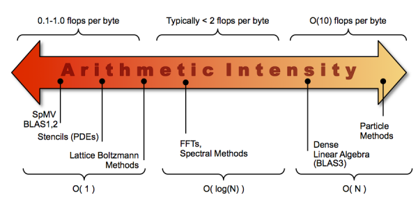 </div>
To put this into perspective in the context of hardware, let’s look at the #3 supercomputer, the Titan system at Oak Ridge National Lab. The GPUs on which it is built (NVIDIA’s K20X) each have a GDDR5-based memory subsystem that can feed the 1.3 TFLOP GPUs at 250 GB/sec. This means that Titan’s FLOPS/byte ratio is around 5.3, or over 4x lower (more balanced) than the 22 FLOPS/byte of TaihuLight’s SW26010 chips.
This huge gap means that an application that is perfectly balanced to run on a Titan GPU–that is, an application with an arithmetic intensity of 5.3–will run 4x slower on one of TaihuLight’s SW26010 processors than a Titan GPU. Put simply, despite being theoretically capable of doing 3 TFLOPS of computing, TaihuLight’s processors would only be able to deliver performance to 1/4th of that, or 0.75 TFLOPS, to this application. Because of the severely limited per-node memory bandwidth, this 93 PFLOP system would perform like a 23 PFLOP system on an application that, given an arithmetic intensity of 5.3, would be considered highly optimized by most standards.
Of course, the indigenous architecture also means that application developers will have to rely on indigenous implementations or ports of performance runtimes like OpenMP and OpenACC, libraries like BLAS, and ISA-specific vector intrinsics. The maturity of this software stack for the ShenWei-64 architecture remains unknown.
<h2>What is interesting</h2>This all isn’t to say that the TaihuLight system isn’t a notable achievement; it is the first massive-scale deployment of a CPU-based manycore processor, it is the first massive-scale deployment of EDR InfiniBand, and its CPU design is extremely interesting in a number of ways.
The CPU block diagrams included in Dongarra’s report are a bit like a Rorschach test; my esteemed colleagues at The Next Platform astutely pointed out its similarities to KNL, but my first reaction was to compare it with IBM’s Cell processor:
<table align="center" cellpadding="0" cellspacing="0" class="tr-caption-container" style="margin-left: auto; margin-right: auto; text-align: center;"><tbody><tr><td style="text-align: center;"> </td></tr><tr><td class="tr-caption" style="text-align: center;">IBM Cell BE vs. ShenWei SW26010. Cell diagram stolen from NAS; SW26010 diagram stolen from the Dongarra report.</td></tr></tbody></table>
The Cell processor was ahead of its time in many ways and arguably the first manycore chip targeted at HPC. It had
<ul><li>a single controller core (the PPE) with L1 and L2 caches</li><li>eight simpler cores (the SPEs) on an on-chip network with no L2 cache, but an embedded SRAM scratchpad</li></ul><div>and by comparison, the SW26010 has</div>
- a single controller core (the MPE) with L1 and L2 caches
- sixty-four simpler cores (the CPEs) on an on-chip network with no L2 cache, but an embedded SRAM scratchpad
Of course, the similarities are largely superficial and there are vast differences between the two architectures, but the incorporation of heterogeneous (albeit very similar) cores on a single package is quite bold and is a design point that may play a role in exascale processor designs:
<table align="center" cellpadding="0" cellspacing="0" class="tr-caption-container" style="margin-left: auto; margin-right: auto; text-align: center;"><tbody><tr><td style="text-align: center;"> </td></tr><tr><td class="tr-caption" style="text-align: center;">What an exascale processor might look like, as stolen from Kathy Yelick</td></tr></tbody></table>
which may feature a combination of many lightweight cores (not unlike the CPE arrays on the TaihuLight processor) and are accompanied by a few capable cores (not unlike the MPE cores).
The scratchpad SRAM present on all of the CPE cores is also quite intriguing, as it is a marked departure from the cache-oriented design of on-package SRAM that has dominated CPU architectures for decades. The Dongarra report doesn’t detail how the scratchpad SRAM is used by applications, but it may offer a unique new way to perform byte-granular loads and stores that do not necessarily waste a full cache line’s worth of memory bandwidth if the application knows that memory access is to be unaligned.
This is a rather forward-looking design decision that makes the CPU look a little more like a GPU. Some experimental processor designs targeting exascale have proposed eschewing deep cache hierarchies in favor of similar scratchpads:
<table align="center" cellpadding="0" cellspacing="0" class="tr-caption-container" style="margin-left: auto; margin-right: auto; text-align: center;"><tbody><tr><td style="text-align: center;"> </td></tr><tr><td class="tr-caption" style="text-align: center;">The Traleika Glacier processor design, featuring separate control and execution blocks and scratchpad SRAM. Adapted from the Traleika Glacier wiki page.</td></tr></tbody></table>
Whether or not we ever hear about how successful or unsuccessful these processor features are remains to be seen, but there may be valuable lessons to be learned ahead of the first generation of exascale processors from architectures like those in the TaihuLight system.
<h2>Outlook</h2>At a glance, it is easy to call out the irony in the U.S. government’s decision to ban the sale of Intel’s KNL processors to the Chinese now that the TaihuLight system is public. It is clear that China is in a position to begin building extreme-scale supercomputers without the help of Intel, and it is very likely that the U.S. embargo accelerated this effort. As pondered by an notable pundit in the HPC community,
<blockquote class="twitter-tweet"><div dir="ltr" lang="en">If US gov hadn’t barred US #HPC tech to China, new No.1 #supercomputer could’ve been #KNL-powered instead of Chinese CPUs? #ISC16 #backfired</div>
— Andrew Jones (@hpcnotes) June 20, 2016</blockquote>
And this may have been the case. However, despite the TaihuLight system’s #1 position and very noteworthy Linpack performance and efficiency, is not the massive disruptor that puts the U.S. in the back seat. Underneath TaihuLight’s shiny, 93-petaflop veneer are some cut corners that substantially lower its ability to reliably deliver the performance and scientific impact commensurate to its Linpack score. As pointed out by a colleague wiser than me, Intel’s impending KNL chip is the product of years of effort, and it is likely that it will be years before ShenWei’s chip designs and fabs are able to be really deliver a fully balanced, competitive, HPC-oriented microarchitecture.
With that being said, TaihuLight is still a massive system, and even if its peak Linpack score is not representative of its actual achievable performance in solving real scientific problems, it is undeniably a leadership system. Even if applications can only realize a small fraction of its Linpack performance, there is a lot of discovery to be made in petascale computing.
Further, the SW201060 processor itself features some bold design points, and being able to test a heterogeneous processor with scratchpad SRAM at extreme scale may give China a leg up in the exascale architecture design space. Only time will tell if these opportunities are pursued, or if TaihuLight follows its predecessors into an existence of disuse in a moldy datacenter caused by a high electric bill, poor system design, and lack of software.